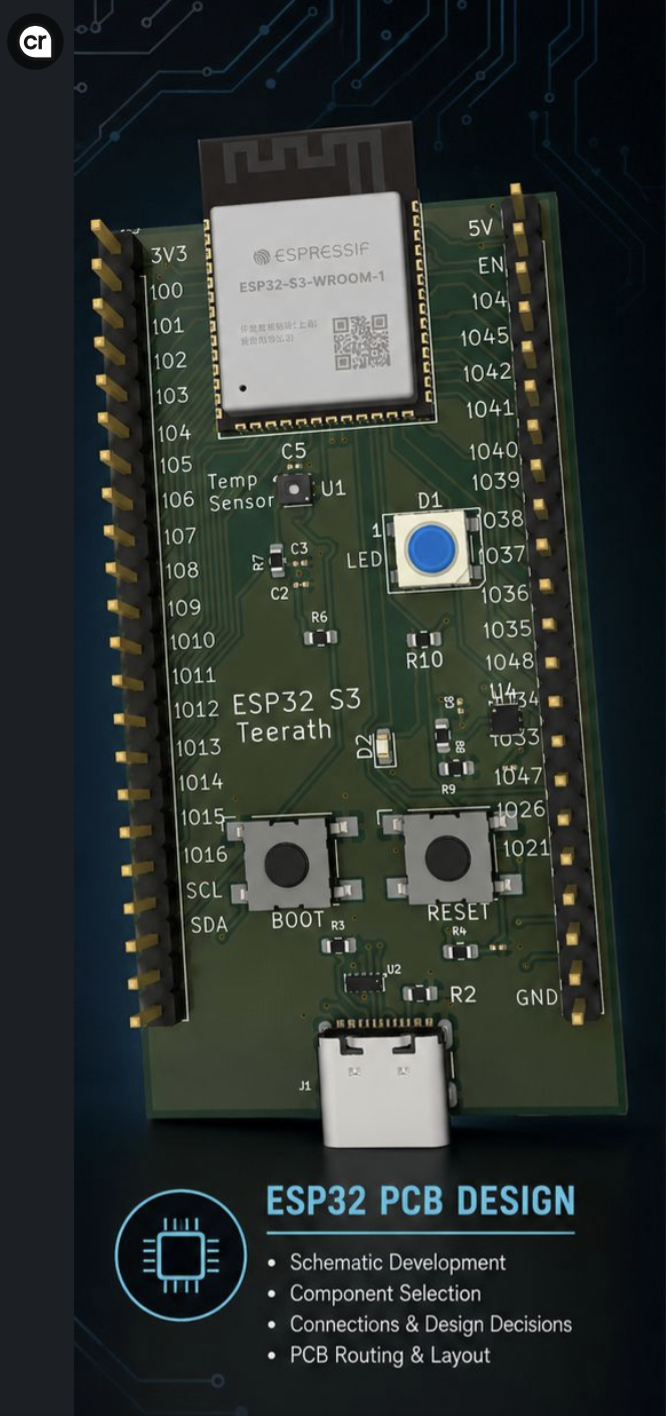
Two independent hardware projects built entirely in KiCad — covering schematic capture, component selection, and full manual routing. The objective across both: move beyond breadboard prototyping and understand every design decision that goes into a fabrication-ready PCB.
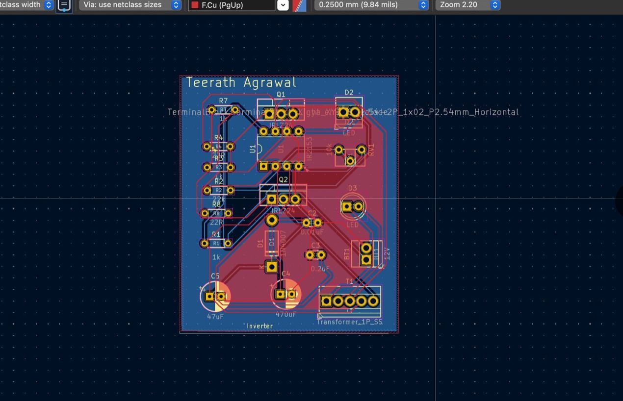
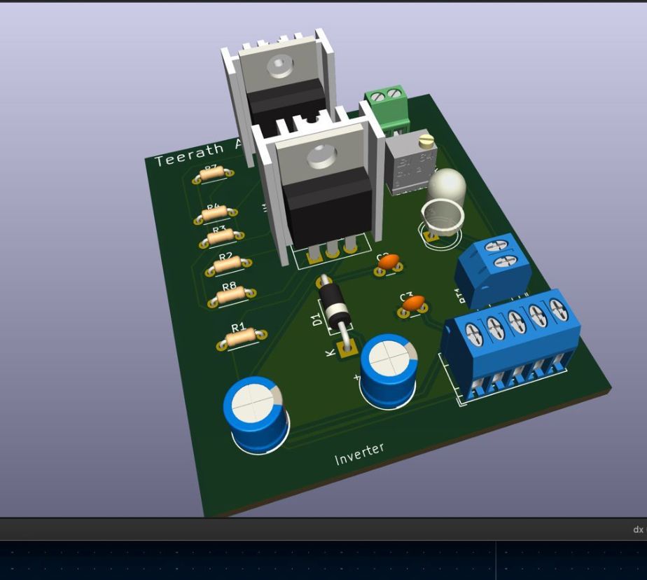
Designed a push-pull DC–AC inverter converting 12V DC to 240V AC via a centre-tapped transformer. Two IRF724 power MOSFETs are driven by a 555 timer oscillator, with gate-drive resistors, a snubber network, and bootstrap capacitors placed to suppress switching transients.
The transformer is mapped to a 5-pin through-hole footprint. Routed on two copper layers with high-current paths kept wide and short — a layout constraint that becomes apparent only when actively working around it to minimise resistive losses and inductive coupling.
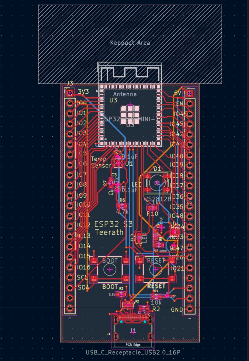
Reverse-engineered the architecture of a standard ESP32-S3 development board and implemented it from scratch in KiCad. The objective was not novelty but comprehension — understanding every design decision embedded in a production-grade MCU carrier board. Autorouting was explicitly discarded; all traces were routed manually.
Net assignment from MCU pads to GPIO headers was iterated multiple times to keep trace lengths short and minimise layer transitions. Via placement required careful layer planning to avoid clearance violations — a process that exposed the real complexity behind what appears, on the surface, to be a simple breakout board. The schematic covers USB-C input, TVS diode ESD protection, LDO 5V–3.3V regulation, per-IC decoupling, GPIO headers, BOOT/RESET logic, and a WS2812B addressable LED.